
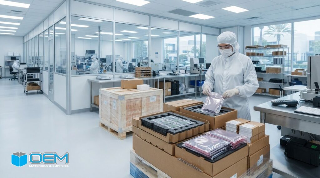
A package that cushions a semiconductor component can still expose it to particle contamination or electrostatic discharge. For Orange County manufacturers, choosing cleanroom packaging for semiconductors means matching materials and design to each handling stage, from controlled production areas to storage and shipment.
Physical protection is only one part of the decision. The right package also depends on facility procedures, ESD risk, product geometry, and how packaging moves through your operation. A mismatch can complicate handling or leave sensitive components exposed.
This guide explains how to define requirements before sourcing and compare options against contamination controls, product protection, and production needs. It covers material and design choices, packaging quantities, and supply planning for an Orange County operation. These considerations help engineers, purchasing teams, and operations managers make a more informed decision about cleanroom packaging for semiconductors in Orange County.
Key Takeaways
- Define contamination, ESD, physical protection, and traceability needs separately before selecting packaging.
- Give product-contact packaging, cushioning, and outer shipping protection distinct roles.
- For cleanroom packaging for semiconductors Orange County, compare design support, material coordination, production needs, and supply continuity.
- Document product dimensions, weight, sensitivity, handling stages, and shipping conditions to guide packaging decisions.
- Coordinate custom packaging design, foam, corrugated packaging, and kitting around documented requirements.
What semiconductor cleanroom packaging in Orange County needs to protect
Cleanroom packaging is selected to support controlled handling and protect a product through defined production and distribution steps. There is no single universal specification. The appropriate design depends on the item, facility procedures, product sensitivity, and how the package will be handled.
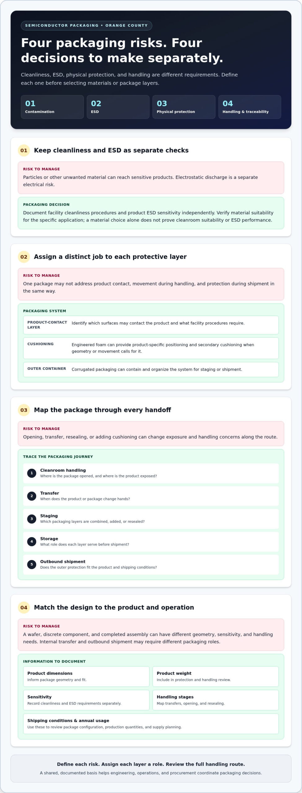
Cleanroom packaging for semiconductors used by Orange County manufacturers should be defined by the risks it needs to manage. Contamination control concerns particles or other unwanted material reaching sensitive products. Electrostatic discharge (ESD) is a separate electrical risk. Physical protection addresses impact, pressure, vibration, or movement. Traceability helps teams identify and track products through defined process steps. One package may need to address several needs, but each should be evaluated separately.
Requirements can change with the product and packaging stage. A wafer, a discrete component, and a completed assembly have different geometries and handling needs. Packaging for an internal transfer may not need to perform the same role as the outer protection used for outbound shipment. Teams assessing cleanroom technology and standards should distinguish facility environmental controls from the packaging decisions made for each product and process.
Separate cleanliness requirements from ESD protection
Cleanroom cleanliness and ESD protection address different hazards. Facility procedures, product sensitivity, and the point of packaging in the workflow should guide material and design requirements. Do not treat a material choice as proof of cleanroom suitability or ESD performance without application-specific verification. Record these requirements separately so the packaging review addresses each risk directly instead of relying on broad assumptions.
Map the packaging journey from production to shipment
Trace the complete route: cleanroom handling, transfer, staging, storage, and outbound shipment. At each step, document where packaging is opened, where the product changes hands, whether the package is resealed, and when cushioning or an outer container is added. These handoffs can introduce different contamination, damage, or handling concerns.
For Orange County operations, align packaging supply with how materials move between production, warehouse, and shipping areas. Packaging design can account for product geometry and those handling steps. For example, custom foam packaging can provide secondary cushioning while a separate package serves the product-contact role. Mapping the journey helps teams specify each layer and coordinate packaging quantities with production and shipment needs.
How semiconductor packaging materials affect contamination and product protection
Packaging materials work as a system. The product-contact layer, cushioning, and outer shipping container each serve a distinct purpose, so no single material is a universal solution. Selection depends on product sensitivity and handling conditions. Orange County manufacturers evaluating cleanroom packaging for semiconductors should define the function of each layer before choosing materials.
Start by identifying which surfaces may contact the product and what facility procedures require. Then assess the protective layers around it. A design that limits movement during shipment also needs to account for how the product is handled when packaging is opened or transferred. Material choice, package geometry, and handling procedures must work together to reduce risk.
Where foam and corrugated packaging can fit
Engineered foam can provide cushioning and product-specific positioning when the product’s shape or movement calls for it. Its design can be coordinated with product geometry and handling steps. Custom foam packaging can serve as a secondary protective layer rather than replacing the product-contact package.
Corrugated packaging can provide an outer protective format for staging or shipment. It contains and organizes the packaging system, while foam or other cushioning materials address movement and contact within it. The right combination depends on the product, shipping conditions, and package configuration. Do not assume a material is suitable for cleanroom use or provides a particular level of ESD protection without application-specific specifications.
Account for ESD, particles, and packaging interfaces
Document the facility’s cleanliness procedures and the product’s ESD sensitivity as separate requirements before selecting materials. Consider each interface: where packaging is opened, where the product is exposed, and whether packaging layers are transferred, combined, or resealed. These transitions can affect handling and exposure, even when the outer package is designed for shipment.
For semiconductor manufacturers in Orange County, follow the product through each packaging layer and handoff. Record which layer contacts the product, what cushioning is added, and how the outer container is used. This gives engineering, operations, and procurement a shared basis for reviewing the design and coordinating material supply.
How to compare cleanroom packaging suppliers in Orange County
Supplier comparisons should look beyond the material itself. Assess how packaging design, production support, and replenishment fit your product and operation. For cleanroom packaging for semiconductors in Orange County, define the project scope with product dimensions, weight, sensitivity, handling stages, and annual usage. These details help align design decisions with production quantities and supply planning.
| Comparison area | Required capability | Project-dependent consideration |
|---|---|---|
| Design and material coordination | Translate product and handling requirements into a packaging design | Whether custom foam, corrugated packaging, or a combination suits the application |
| Production support | Coordinate packaging quantities with the production program | Prototype review, revisions, and expected order patterns |
| Workflow integration | Connect packaging with handling and shipping steps | Whether kitting or assembly can support the packing sequence |
| Supply continuity | Plan replenishment around usage and inventory needs | Whether vendor-managed inventory or just-in-time delivery fits the operation |
Evaluate packaging design and production support
OEM Materials & Supplies develops custom packaging around product geometry and operational requirements. Design discussions can account for how a component is positioned, protected, packed, and prepared for shipment. Prototype review can help teams assess fit and handling before moving into a production program. Explore custom packaging design as part of the evaluation.
For a useful review, bring drawings or dimensions, product weight, handling steps, annual usage, and shipping conditions. This gives engineering, procurement, and operations a common project basis. Kitting and assembly can also organize packaging components to support the packing workflow.
Compare supply continuity for Orange County operations
Replenishment planning connects packaging consumption with production schedules and inventory levels. Vendor-managed inventory and just-in-time delivery are coordination approaches that can be structured around an operation’s needs. They are not guarantees against shortages. Their usefulness depends on accurate usage information and a workable replenishment plan.
For Orange County manufacturers, review how order patterns, storage capacity, and delivery coordination fit the local production workflow. OEM Materials supports packaging supply planning through vendor-managed inventory and just-in-time delivery. Share your product dimensions, weight, and annual usage to discuss packaging requirements and supply coordination.
A practical evaluation process for Orange County semiconductor packaging
A documented review helps engineering, operations, and purchasing teams evaluate the same requirements before packaging moves into production. Use this workflow to connect product protection with operator handling and supply planning for semiconductor operations in Orange County.
- 1. Build the requirement brief. Record product dimensions, weight, geometry, fragility, and sensitivity to ESD or contamination. Note packing quantities, annual usage, shipping conditions, and facility procedures that affect packaging.
- 2. Map the handling steps. Identify where packaging enters the process, where it is opened or transferred, and how operators handle it before shipment. Include handoffs between production, staging, storage, and shipping.
- 3. Define packaging roles. Separate product-contact packaging from cushioning and outer protection. Document what each layer needs to do, then align material and design decisions with the product and its journey.
- 4. Review the design and sample. Evaluate fit, access, operator handling, and packing sequence. Sample review can reveal interference, unnecessary handling, or poor fit before a design enters a production program.
- 5. Plan quantities and replenishment. Consider production volume, storage constraints, order patterns, and replenishment preferences. Establish how packaging needs will be coordinated as the program runs.
Build a packaging requirement brief
Keep the brief specific and usable. Include product drawings or measurements where available, weight, sensitivity, packing quantities, and a description of each handling stage. Document relevant facility requirements and procedures. If the project specifies a cleanroom or ESD standard, verify its applicability and supporting material specifications before including it in the package requirements. This prevents assumptions from becoming unsupported performance claims.
Review samples, workflow, and replenishment needs
During sample review, have the people who pack or handle the product walk through the actual sequence. Check whether the product fits as intended, whether operators can access and secure it efficiently, and whether packaging components are organized for the task. Then compare the proposed approach with production volume, available storage, and replenishment preferences.
For semiconductor packaging programs in Orange County, coordinate design and supply planning with the production program. Cost and labor outcomes depend on product dimensions, selected materials, and shipping requirements. Request a project quote with product dimensions, weight, handling steps, and annual usage to support a focused packaging review.
Partner with OEM Materials & Supplies for semiconductor packaging in Orange County
Semiconductor packaging decisions need to work for both the product and the production program. OEM Materials & Supplies serves manufacturers in Orange County and throughout Southern California with custom packaging design, engineered foam packaging, corrugated boxes, kitting, assembly, and inventory support. The goal is to align the packaging system with documented product, handling, and shipping requirements, not assume a single format fits every application.
For teams evaluating cleanroom packaging for semiconductors in Orange County, start with a clear definition of what the package must protect, how operators use it, and where packaging enters the workflow. Product geometry, handling steps, packaging stages, and shipping conditions help guide design decisions. Document cleanliness or ESD requirements separately and address them using verified material specifications, rather than assuming performance from a general material description.
Coordinate packaging design with production requirements
Custom packaging design brings product protection and packing workflow into the same review. Engineered foam can provide cushioning or product-specific positioning, while corrugated packaging can serve as an outer container. The right combination depends on the project. Explore foam packaging options as part of a broader review of package layers, operator handling, and shipping needs.
Kitting and assembly can organize packaging components to support the production or packing sequence. Reviewing these needs together helps teams consider the complete workflow, from packaging preparation to outbound shipment, rather than treating each material as a separate purchasing decision.
Prepare information for a useful packaging quote
A well-defined project brief makes packaging discussions more practical. Include product dimensions and weight, annual usage, relevant handling requirements, and the stages where packaging is opened, transferred, or combined with other materials. Shipping conditions, production quantities, storage constraints, and replenishment preferences can further inform design and supply planning.
For Orange County manufacturers, vendor-managed inventory or just-in-time delivery can help coordinate packaging replenishment with operational needs. The appropriate approach depends on usage patterns and the production program. Share your requirements with OEM Materials & Supplies to evaluate custom packaging, foam, corrugated options, and related supply needs.
Request a packaging quote and include product dimensions, weight, annual usage, handling stages, and shipping conditions to support a focused project review.
Build a Packaging Plan Around Your Production Needs
Effective semiconductor packaging starts with clearly defined requirements. Separate contamination controls, ESD concerns, physical protection, and traceability, then map how each package will be handled from production through shipment. Material and design choices should match the product, workflow, and shipping conditions rather than rely on a universal solution.
For cleanroom packaging for semiconductors in Orange County, OEM Materials & Supplies helps manufacturers coordinate custom packaging design and production needs. Foam packaging and corrugated boxes can be evaluated alongside kitting, assembly, and inventory services to support a practical packaging program. Any cost or labor benefits depend on product dimensions, selected materials, and shipping requirements.
Share your product dimensions, weight, annual usage, handling stages, and shipping conditions to begin a focused review. Request a packaging quote and put a clear plan in motion with a packaging partner serving Orange County and Southern California.
Frequently Asked Questions
What is cleanroom packaging for semiconductors?
Cleanroom packaging for semiconductors is selected to support controlled handling and protect sensitive products through defined production, storage, and shipping steps. Requirements depend on the component, facility procedures, and packaging stage. Consider contamination control, electrostatic discharge (ESD), physical protection, and traceability as separate but related needs. No single packaging format or material should be assumed to meet every facility or product requirement.
How do I choose packaging for semiconductor components handled in a cleanroom?
Start with the component’s dimensions, weight, sensitivity, and handling path. Document where packaging is opened, transferred, or resealed, along with facility cleanliness procedures, ESD concerns, and shipping conditions. Then evaluate each layer by function: product-contact packaging, cushioning, and the outer shipping container. For cleanroom packaging for semiconductors in Orange County, these details help align design and supply planning with your production workflow.
Can corrugated boxes be used for semiconductor cleanroom packaging?
Corrugated boxes can serve as outer protective or shipping packaging, but their role should be distinguished from product-contact packaging used during controlled handling. Consider where the box enters the process, where it will be opened, and whether it could introduce particles into a controlled area. The right design depends on facility procedures and the application. Do not assume corrugated packaging is suitable for every cleanroom stage without review.
How does ESD protection differ from cleanroom packaging?
ESD protection addresses the risk of electrostatic discharge damaging sensitive electronic components. Cleanroom packaging concerns handling and contamination-control requirements. A package may need to address both, but one does not automatically provide the other. Document product sensitivity and facility procedures separately, then evaluate relevant material specifications for the application. A general “cleanroom” or “antistatic” description does not establish a particular level of performance.
What information should I provide when requesting a semiconductor packaging quote?
Provide product dimensions, weight, annual usage, and any drawings or descriptions that clarify product geometry. Include sensitivity to ESD or physical damage, handling steps, packaging stages, and shipping conditions. Note production quantities, storage constraints, and replenishment preferences as well. For manufacturers in Orange County, Los Angeles, San Diego, or Riverside, this information helps connect packaging design and supply planning to the operation’s requirements.
How can packaging design reduce handling and shipping damage?
Packaging design can position a product appropriately, limit unwanted movement, and organize materials around the operator’s packing sequence. Reviewing a sample with the people who handle the product can reveal fit, access, or workflow issues before a design enters production. Foam packaging can provide cushioning, while a corrugated box can serve as an outer container. Results depend on product dimensions, materials, handling, and shipping requirements.
Does OEM Materials serve semiconductor manufacturers in Orange County?
Yes. OEM Materials & Supplies serves manufacturers in Orange County and throughout Southern California, including Los Angeles, San Diego, and Riverside. The company supports custom packaging design, foam packaging, corrugated boxes, kitting, assembly, and inventory programs. Packaging recommendations are based on documented product, handling, and supply needs, helping teams coordinate design decisions with production and shipping workflows.