

Electrostatic discharge (ESD) can damage sensitive electronic components, and packaging failures often involve gaps in protection during handling, storage, or shipping. Troubleshooting ESD packaging failures in electronics starts with tracing where components may have been exposed to charge.
Packaging is a critical part of an ESD investigation, but it cannot control every source of static on its own. ESD can cause immediate or latent component damage, and parts can become exposed to charge during handling and transit. A practical investigation traces the failure, identifies gaps in protection, and checks whether packaging materials and handling methods suit the component’s sensitivity and shipping conditions.
Key Takeaways
- Trace possible charge exposure across handling, storage, and transit instead of treating packaging as the only potential failure point.
- Match protective packaging to component sensitivity, and distinguish static-control materials from shielding materials.
- Review carts and transfer steps for charge buildup, especially when components are removed from packaging or placed on a workbench.
- Use cushioning and a suitable outer container to address physical shipping hazards without compromising ESD protection.
- Replace static-generating materials near exposed electronics with packaging selected for the component and the handling environment.
1. What damage does static electricity cause to electronic components?
An electrostatic discharge can damage electronic components without a visible spark. An event of 30 volts can permanently damage sensitive parts. The U.S. Environmental Protection Agency says electrostatic discharge can disturb or damage a device’s internal circuitry. A discharge may pass from a charged surface into a component through a connector, contact, or exposed circuit path.
Damage can be immediate, latent, or performance-related. Immediate damage may leave a component unable to start, communicate, or complete a test. Performance-related damage can appear as intermittent resets, signal errors, or unstable operation, depending on which internal circuit was affected. ESD is attributed to more than 25% of electronics failures, and the fault may not be obvious during initial inspection.
Latent damage is harder to trace. The component may pass manufacturing testing, then fail after installation or during service. Over 60% of ESD failures are not detected during manufacturing testing. Latent ESD damage can reduce mean time between failures by up to 50%, and latent failures can cost up to 10× more than catastrophic ESD failures. A device that works after unpacking can still carry hidden damage.
For electronic component packaging, ANSI/ESD S541-2026 is identified as a packaging standard by the EOS/ESD Association. ANSI/ESD S20.20 and IEC 61340-5-1 support an ESD control program. These standards address different parts of the control system; packaging selection should align with the component’s sensitivity and handling process.
Not every shipping failure is electrical. Vibration during transport can loosen connectors, stress solder joints, or let a board strike its enclosure. For example, a poorly restrained circuit board can move inside a box even when its ESD bag remains intact. Foam packaging can cushion and restrain components, but cushioning does not replace static-control packaging. Investigate electrical and mechanical damage as separate failure paths.
When troubleshooting ESD packaging failures in electronics, compare the component’s symptoms with its packing and handling sequence. Record whether the failure is immediate, intermittent, or delayed. Inspect exposed contacts, connector pins, and board edges for physical damage, then review how the item was removed from protective packaging. Match test results to the point when the device’s condition changed. This gives you a clearer basis for correcting packaging or handling steps.
2. What does ESD mean in the supply chain?
Common causes of ESD packaging failures include static-generating materials, opening protective packaging outside controlled work areas, and transferring components without grounding procedures. Protection can also be bypassed during inspection, repacking, or delivery. The risk follows circuit boards through every handoff, not just along the manufacturing line.
In a warehouse, exposure points include receiving, put-away, picking, and staging. A circuit board may move from protective packaging into an ordinary tote at each step. If staff open the package at an uncontrolled station, a discharge can reach exposed contacts. Map each handoff, then identify where components leave protective packaging and where they wait before the next operation.
Transport adds both electrostatic and physical stress. A typical shipping cycle exposes packages to dozens of drops, while vibration and repeated movement can shift components or damage their protective layers. A sealed package can still fail if rough handling tears its bag or pushes the contents against a damaged enclosure. Inspect packaging at dispatch and receipt, and record crushed corners, punctures, or loose closures.
Off-site handling creates a separate control challenge. A service technician may open a package at a customer facility without the same grounded workstation used in manufacturing. Before exposing a board, establish an ESD-controlled work area and follow the component’s handling procedure. Wrist straps include a 1 MΩ resistor, which allows charge to dissipate safely while protecting the operator from shock hazards. The strap works as part of a grounded system, not as a substitute for suitable packaging.
Reusable containers need their own inspection step. A container that carried protected circuit boards on one route may return with contamination, damaged closures, or an unidentified liner. Check its condition and intended use before placing components inside. Assign reusable transport containers to defined packaging tasks, and keep them separate from containers used for general warehouse items.
To trace a supply-chain failure, compare the item’s condition at each transfer point. Note who opened the package, where it was opened, and whether the board remained protected. Compare dispatch and receiving records with the shipment’s packaging condition. This timeline can help distinguish a handling gap from shock damage during transit.
Maintain anti-static precautions during transport, handling, and storage so components receive consistent protection throughout the supply chain. Treat these stages as connected parts of the process, not isolated tasks, and keep the precautions in place at every handoff.
3. ESD-safe storage and shipping packaging
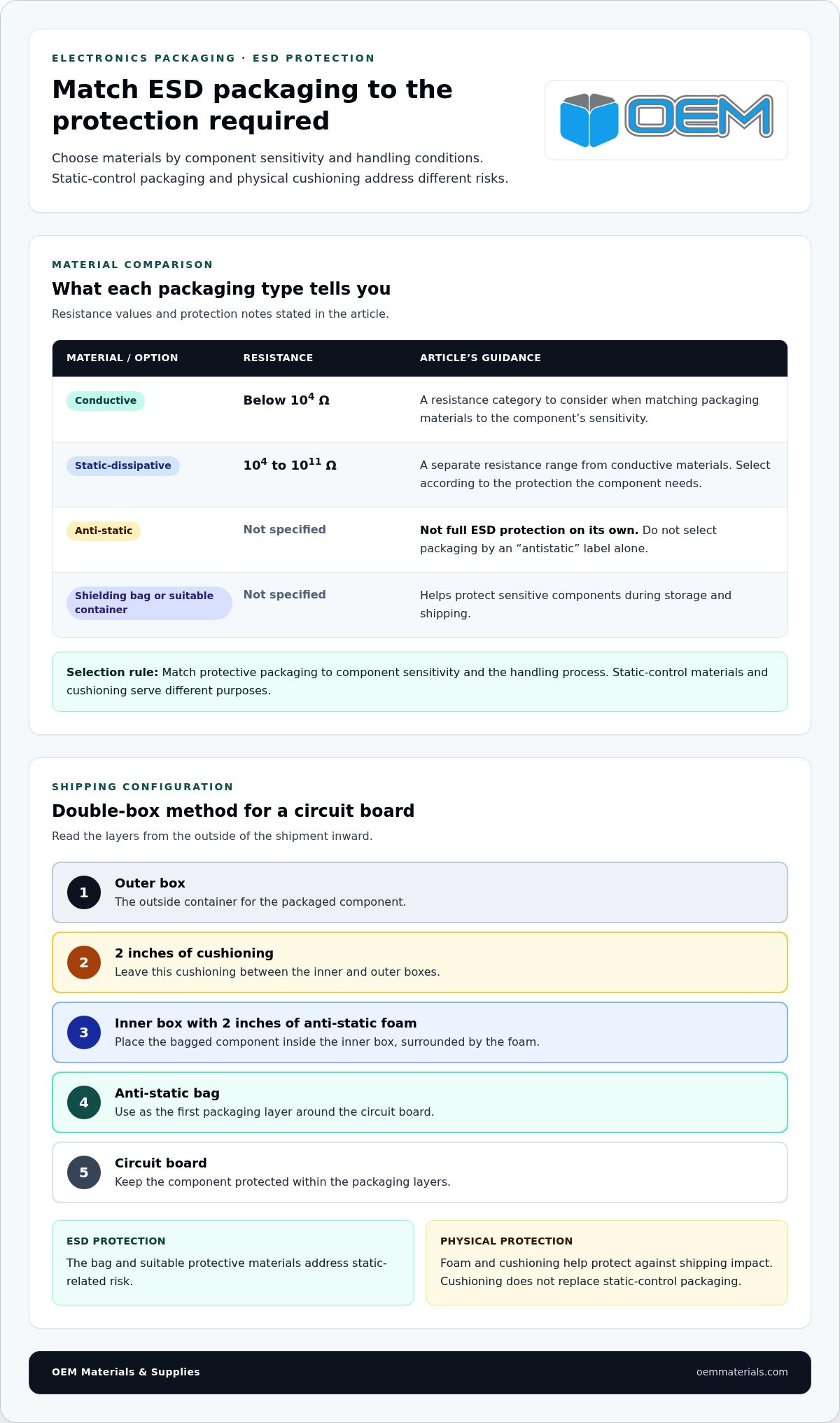
Choose packaging by the protection the component needs, not by an “antistatic” label alone. Conductive materials have resistance below 104 ohms; static-dissipative materials range from 104 to 1011 ohms. Anti-static packaging alone does not provide full ESD protection. A shielding bag or suitable container helps protect sensitive components during storage and shipping.
For circuit boards with exposed electronics, use an anti-static bag as the first packaging layer. A double-box method places the bagged component inside an inner box, surrounded by 2 inches of anti-static foam, then leaves 2 inches of cushioning between the inner and outer boxes. This separates static protection from impact protection.
Pink anti-static bags are recommended for most applications, while silver metalized static-shielding bags provide Faraday cage protection. Conductive foam can protect exposed leads, and ESD-safe sheets or wraps can separate items inside a container. Avoid placing regular bubble wrap directly against a circuit board. Select materials based on contact points, component sensitivity, and how the package will move in transit.
To verify whether bags, trays, foam, and cushioning suit sensitive electronics, review their resistance and intended protective function against the component’s handling requirements. Inspect seals, closures, surfaces, and cushioning for tears, contamination, or wear. The National Bureau of Standards advises checking antistatic protective measures, including conductive packaging, for effectiveness.
Inspect packaging at receipt, before reuse, and before packing a shipment. Keep records of material identification, inspection results, damage, replacement, and the shipment or storage location. IEC 61340-5-1 can guide documentation of packaging requirements within an ESD control program; ANSI/ESD S541-2026 is identified as a packaging standard within such a program by the EOS/ESD Association.
Use an ESD-protected work area for opening, repacking, or inspecting exposed components. IEC 61340-5-1 provides a framework for an ESD Protected Area, while grounded benches and mats help control charge at workstations. Ionizers can help neutralize charge on isolated objects that cannot be grounded, but they do not replace suitable packaging or grounding practices.
For reliable storage, keep components inside closed protective packaging until they reach an ESD-controlled station. Document the packaging configuration alongside component and shipment records. If a package is opened for inspection, restore the specified protection before storage or transport, and record any material change.
4. Charge buildup on carts and safe package handling
A warehouse cart can become a charge source when its wheels, surface, or load generate static during movement. In one described cart scenario, the cart and employee build up a charge of 10 kV. Bringing that charge near an exposed circuit board creates a discharge path. The package may look intact, yet the handling transfer can still expose components to ESD damage.
Control the transfer, not just the package. Keep the component inside its shielding bag while moving it between work areas. Place the sealed package on the ESD bench before opening it. Avoid dumping components onto the bench, where sudden contact can cause rapid discharge. Let the package and work surface equalize through the controlled setup.
Packaging can generate charge during removal. Removing a PCB from non-antistatic packaging can generate 12,000 V. Regular bubble wrap placed directly against a circuit board can generate charges exceeding 10,000 volts. Keep ordinary bubble wrap, plastic, and other static-generating materials away from exposed electronics. Use them only outside the suitable ESD protection layer.
Shielding works only as part of a handling system. ESD shielding bags protect components when sealed and properly grounded within that system. Opening a bag beside an ungrounded cart or ordinary plastic tote can undo the protection at the point of access. Keep bags closed until the item reaches the designated ESD work area, and reseal components before moving them again.
Labels support consistent handling, but they do not dissipate charge or shield a component. Use package labels to identify ESD-sensitive contents and communicate handling steps. For example, a label can tell receiving staff to keep the bag sealed until it reaches an ESD-controlled station. Match the label to the contents and packing configuration.
During troubleshooting, trace each movement from storage to bench. Record whether staff used a cart, opened the package, or transferred the component to another container. Inspect the bag for punctures and check whether the item remained sealed during movement. Compare these observations with the failure location to find where shielding or handling controls broke down.
Standardize the procedure for operators and delivery teams: keep sensitive components packaged, use designated transfer equipment, and open shielding only at a controlled workstation. Train staff to recognize ESD labels and protect packages during handoffs. Consistent procedures make deviations visible, helping teams isolate charge buildup instead of replacing packaging without finding the cause.
5. Material selection based on component sensitivity
Start material selection with the component’s ESD sensitivity, exposed features, and physical shape. GaAs devices often require Class 0 handling procedures because of their low tolerance levels. HBM Class 0 components have a sensitivity threshold below 125 V. Use the component’s sensitivity classification to define the protection required during production, inspection, and storage.
Next, map the component’s geometry. Identify exposed leads, connector pins, board edges, and areas that must not bear pressure. A tray should locate the part without allowing it to shift, while an insert should support stable surfaces rather than delicate contacts. For example, a board with protruding connectors needs clearance around those features and restraint at stronger support points.
Package fit affects electrical protection and physical condition. An oversized cavity allows movement in transit; a tight fit can press on connectors or bend leads. Match the cavity, support points, and access method to the item’s orientation and removal sequence. For assemblies with different shapes, separate compartments can reduce contact between components and make consistent placement easier.
Humidity and handling conditions also inform the specification. Dry conditions can increase charge accumulation, while humidity control helps limit that risk. Maintaining relative humidity above 40-60% where practical is recommended as part of ESD control. Record the storage environment and the packaging’s exposure to repeated opening, compression, or surface wear when evaluating performance.
Damaged, counterfeit, or noncompliant packaging may not provide the protection its markings imply. A torn enclosure or poorly fitting insert can leave sensitive areas exposed or allow movement. Inspect materials before use, compare identification and markings with purchasing records, and isolate suspect packaging from production. Keep inspection records and identify affected components to support a focused investigation.
Test-equipment and material costs depend on equipment capability, material type, component geometry, and inspection requirements. The price depends on the specific case and is provided after a quote request. Humidity, handling, and storage conditions affect charge exposure and physical wear, so specify the actual operating environment when selecting materials.
For a packaging recommendation, provide component dimensions, exposed features, storage conditions, and shipping requirements. Request a packaging quote to discuss a configuration suited to the component and its handling path.
Avoid regular plastic, bubble wrap, and Styrofoam for ESD-sensitive products because these materials can generate static charges. Choose suitable ESD packaging instead.
OEM Materials & Supplies: Corrugated Boxes
OEM Materials & Supplies supports the physical protection side of electronics packaging with corrugated boxes, foam packaging, and packaging kits. Corrugated boxes provide an outer shipping container, while a separate ESD-protective layer must protect sensitive components from static discharge. Foam can limit movement and absorb impact when selected to fit the item and package geometry.
Turn to OEM Materials & Supplies when shipment damage points to poor fit, inadequate cushioning, or inconsistent packing materials. Share component dimensions, weight, and shipping conditions to help define a practical packaging configuration. For ESD-sensitive electronics, keep static-control requirements distinct from cushioning requirements so each layer has a clear role.
Contact OEM Materials & Supplies to discuss packaging for your electronics shipments.
Build a More Reliable Packaging Process
Use recurring damage reports to refine packaging specifications and handling procedures. Document what changed, where components were exposed, and which packaging configuration was used. This record gives engineering, operations, and procurement teams a shared basis for evaluating the next shipment. A disciplined approach to troubleshooting ESD packaging failures in electronics can turn isolated incidents into practical process improvements.
OEM Materials & Supplies offers corrugated boxes, foam packaging, and packaging kits for electronics shipments. These materials support the physical packaging plan, while ESD protection must be selected and applied according to component sensitivity. Share your product dimensions, weight, and shipping requirements to help define a suitable packaging configuration.
For a packaging recommendation, request a quote from OEM Materials & Supplies. Each shipment is an opportunity to strengthen handling consistency and protect product condition from packing through delivery.
Frequently Asked Questions
What Is Electrostatic Discharge?
Electrostatic discharge is a sudden movement of electrical charge between objects with different electrical potentials. In an electronics facility, charge can transfer through a person, tool, fixture, or product contact. The path may be brief and invisible, so visual inspection alone cannot establish whether a discharge occurred. Treat ESD as an electrical event to control through the work process, not simply as a packaging label.
What damage does static electricity cause to electronic components?
ESD can cause a component to fail, behave inconsistently, or operate with reduced margin. For a practical comparison, check the affected unit’s test results against its approved acceptance criteria and those of an unaffected unit from the same production lot. Record the specific function that changed, such as an input channel or communication interface. This narrows diagnostic work without assuming every fault has an ESD cause.
How exactly does ESD damage happen?
Damage occurs when discharge current passes through a device structure that cannot tolerate the electrical stress. Current may enter through an external pin and affect an internal junction or circuit path. The component may fail outright, or its electrical characteristics may shift while it continues to operate. The physical damage site and the point where charge entered are not always the same.
Quick Answer: Is ESD Still a Problem Today?
Yes. Modern electronics still require controlled handling because smaller, denser circuits can be sensitive to electrical events. Many modern digital systems operate at 0.7 V to 1.8 V, while a person may not feel an electrostatic discharge until approximately 3,500 volts. That difference means human perception cannot serve as an ESD detection method. Use defined controls and suitable test methods instead.
Where are the hidden ESD risks?
Look beyond packing stations to places where components are briefly exposed: test fixtures, maintenance benches, rework areas, and temporary staging locations. A grounded station can also lose effectiveness if a connection becomes loose or a routine task bypasses the established procedure. Compare work instructions with actual operator movement, including tool placement and component orientation. Small process deviations can reveal more than a visual package inspection.
How do you test ESD packaging for shielding, charge generation, and resistance?
Use a test method suited to the property being evaluated: resistance testing for electrical behavior, charge-generation assessment for material interaction, and shielding testing for protection of the packaged item. Test the finished package as well as representative material, since folds, seams, and closures affect the assembled configuration. Document the equipment, test conditions, sample identification, and result so later evaluations use a comparable method.
What are the acceptable surface resistance ranges for ESD packaging materials?
Conductive packaging materials have resistance below 104 ohms, while static-dissipative materials range from 104 to 1011 ohms. These categories describe material behavior, but a resistance result alone does not establish that a package provides the protection a specific component needs. Apply the packaging specification and component sensitivity requirements when interpreting the measurement and approving a material.
How can you troubleshoot ESD damage found after shipping or receiving?
Place potentially affected units on hold and preserve the shipment’s packaging configuration for investigation. Compare the received or returned unit with an unaffected unit using the same approved functional test. Review handling records alongside component lot and package identification, then determine whether affected parts share a route, material batch, or packing step. This evidence helps teams define a targeted corrective action rather than changing several controls at once.