
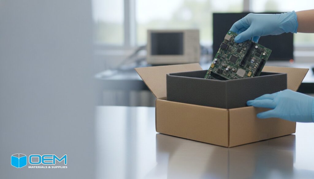
A single electrostatic discharge event can render a high-value circuit board useless before it even reaches your customer, yet many manufacturers still rely on generic cushioning instead of custom die cut inserts for electronics. It’s clear that high damage rates and inefficient manual packing processes are more than just logistical hurdles; they represent a direct hit to your company’s profitability and reputation. Relying on oversized boxes and excessive filler also creates unnecessary waste that complicates your compliance with evolving environmental standards.
This engineering guide explains how to design these specialized inserts to eliminate shipping damage while optimizing assembly through precision kitting. You’ll learn how to select materials that provide both physical shock absorption and shielding to meet the latest ANSI/ESD S541-2026 requirements. We also address how Southern California operations in Orange County and Los Angeles are maintaining compliance with California SB 54 plastic regulations while achieving zero-damage shipping cycles for their most sensitive components. This overview provides the technical context needed to transition from basic packaging to an engineered protection system.
Key Takeaways
- Learn how to select the optimal material density, balancing foam and corrugated options to protect high-value components from physical impact.
- Understand the engineering requirements for custom die cut inserts for electronics to ensure compliance with ANSI/ESD S541-2026 static protection standards.
- Discover how precision insert design reduces labor costs by streamlining the packing process and facilitating efficient kitting services.
- Stay ahead of California SB 54 regulations by integrating sustainable, recyclable materials into your engineered packaging solutions.
- Optimize your supply chain with Southern California sourcing strategies like vendor-managed inventory and just-in-time delivery for factories in Los Angeles and Orange County.
Understanding Custom Die Cut Inserts for Electronics
Precision is the baseline requirement for electronics manufacturing. When shipping high-value circuit boards or sensitive sensors, a generic box filled with loose-fill material is rarely sufficient. Die cutting is a fabrication process that utilizes a customized steel rule die to shear, shape, and cut materials like foam or corrugated fiberboard into exact profiles. For industrial electronics, this process transforms raw material into a functional component of the product’s protection strategy. These inserts serve as a rigid internal skeleton that eliminates the movement responsible for most transit-related failures.
Electronics require much tighter tolerances than general consumer goods. A shift of even a few millimeters can lead to abrasion against a connector or a cracked solder joint. Using custom die cut inserts for electronics allows engineers to design “lock-and-key” fitments that secure every component in a fixed position. This level of control replaces inefficient materials like packing peanuts or crumpled paper, which settle during transit and leave products vulnerable to impact. By switching to engineered inserts, manufacturers in Southern California hubs like Orange County and Los Angeles often see a drastic reduction in both shipping damage and the volume of packaging waste generated.
The Mechanics of Die Cutting
The steel rule die process is the industry standard for high-speed, high-accuracy production. A die is constructed by embedding sharp steel blades into a laser-cut wooden base, which is then used to stamp out shapes with repeatable precision. This method is ideal for creating complex custom foam packaging that mirrors the intricate geometry of a PCB assembly. While simple dividers only provide basic separation, multi-layered inserts can be engineered to provide varying levels of compression and shock absorption. This ensures that the most delicate parts of the device never make contact with the outer walls of the shipping container.
When to Move from Stock to Custom
Identifying the right time to invest in custom tooling is a matter of calculating the total cost of ownership. Many operations reach a tipping point where the cost of product returns and the labor spent on “wrapping and taping” exceeds the initial investment in a custom die. If your warehouse team spends more than thirty seconds securing a single unit with bubble wrap, you’re likely losing money on labor. Moving to a custom packaging design allows for rapid kitting, where parts simply snap into place. This transition is especially valuable when scaling from prototypes to high-volume production runs, as it standardizes the protection level across every unit shipped from your facility.
Material Selection: Foam vs. Corrugated Inserts
Selecting the right material for custom die cut inserts for electronics involves balancing the product’s fragility rating, or G-factor, against its total mass. Heavy industrial power supplies require high-density support to prevent “bottoming out” during a drop, while lightweight sensors need soft cushioning to decelerate impact safely. Thermal management also plays a role in selection. Foam acts as an effective insulator, which helps protect temperature-sensitive components when shipments sit on a hot tarmac or in a cold freight container.
Environmental compliance is now a critical engineering constraint for manufacturers in the Inland Empire and San Diego. Under California SB 54, 100% of single-use packaging sold in the state must be recyclable or compostable by 2032. This mandate is pushing many electronics firms to re-evaluate their reliance on non-recyclable plastics. Integrating specialized inserts with corrugated boxes creates a high-performance solution that meets both protection requirements and strict sustainability goals. Choosing the right material mix ensures you aren’t just protecting the product, but also future-proofing your supply chain against regulatory penalties.
Engineered Foam Materials
The choice between Polyethylene (PE) and Polyurethane (PU) depends on the item’s weight and the likelihood of repeated impacts. PE is a closed-cell foam that provides excellent support for heavier electronics and naturally resists moisture. For the aerospace and medical device sectors, cross-linked polyethylene (XLPE) is often the standard. It offers a high-purity, non-abrasive surface that’s compatible with cleanroom environments. PU is an open-cell foam, making it better for very light, highly fragile items that require a soft landing. Density ratings are vital; a foam that’s too dense won’t compress enough to protect a light circuit board, while a foam that’s too soft will fail to support a heavy metal chassis.
Corrugated Die-Cut Solutions
Corrugated fiberboard provides structural rigidity and weight distribution for components that don’t require the extreme cushioning of foam. These inserts are highly effective for securing cables, metal housings, or mounting hardware within a larger kit. They are typically more cost-effective for high-volume production and are easily recycled by the end user. Many sophisticated designs utilize a hybrid approach. This uses a corrugated frame for structural integrity combined with foam pads at specific contact points where the sensitive circuitry touches the packaging. This method minimizes material use while maximizing protection. If you’re unsure which material density fits your product’s specific G-factor requirements, you can request a quote and material analysis to ensure your design is mathematically sound.
Protecting Sensitive Circuitry: ESD and Shock Absorption
Friction within a shipping container is a primary source of electrostatic discharge (ESD), a hidden threat that can destroy microprocessors and sensors without leaving visible marks. In the industrial supply chain, triboelectric charging occurs whenever materials rub together during transit. According to the ANSI/ESD S541-2026 standard, packaging for items shipped outside of an ESD Protected Area must provide both antistatic and shielding protection. Standard pink antistatic materials are often insufficient on their own because they do not shield against external electric fields. This is why custom die cut inserts for electronics are frequently engineered using specialized dissipative or conductive grades to ensure comprehensive safety.
Identifying which components require this level of protection is essential for cost-effective engineering. Integrated circuits, MOSFETs, and medical diagnostic sensors are particularly vulnerable to low-voltage events. For the semiconductor and medical device sectors, material selection must also account for cleanroom compatibility. Standard foams can slough particles or outgas chemicals that contaminate sensitive surfaces. Utilizing high-purity, non-sloughing materials ensures that your packaging doesn’t introduce new failure points. For a deeper look at specific material properties and technical specifications, refer to our industrial guide to foam inserts.
Anti-Static and Dissipative Materials
There’s a significant functional difference between pink anti-static foam and black conductive foam. Pink foam is topically treated with antistatic agents that prevent the generation of static, but these chemicals can migrate or lose effectiveness in low-humidity environments. Black conductive foam is carbon-loaded, providing a permanent path for charges to dissipate safely. Engineers typically look for surface resistivity measurements between 10^4 and 10^11 ohms per square to categorize a material as dissipative. Choosing the correct grade ensures long-term stability during extended storage in warehouses across the Inland Empire or San Diego County.
Engineering for G-Force Protection
Protecting electronics from physical impact requires calculating the specific drop height requirements based on the shipping environment. Most industrial standards, such as ISTA testing, simulate drops from 36 to 48 inches. Custom die cut inserts for electronics use precise geometry to distribute this impact energy away from critical solder joints and toward the sturdier parts of the device housing. This prevents the “bottoming out” effect where the foam fully compresses and transfers the shock directly to the component. The specific cell structure of the foam, whether open or closed, dictates how effectively the material absorbs high-frequency vibrations that can loosen internal connectors during long-haul transit.
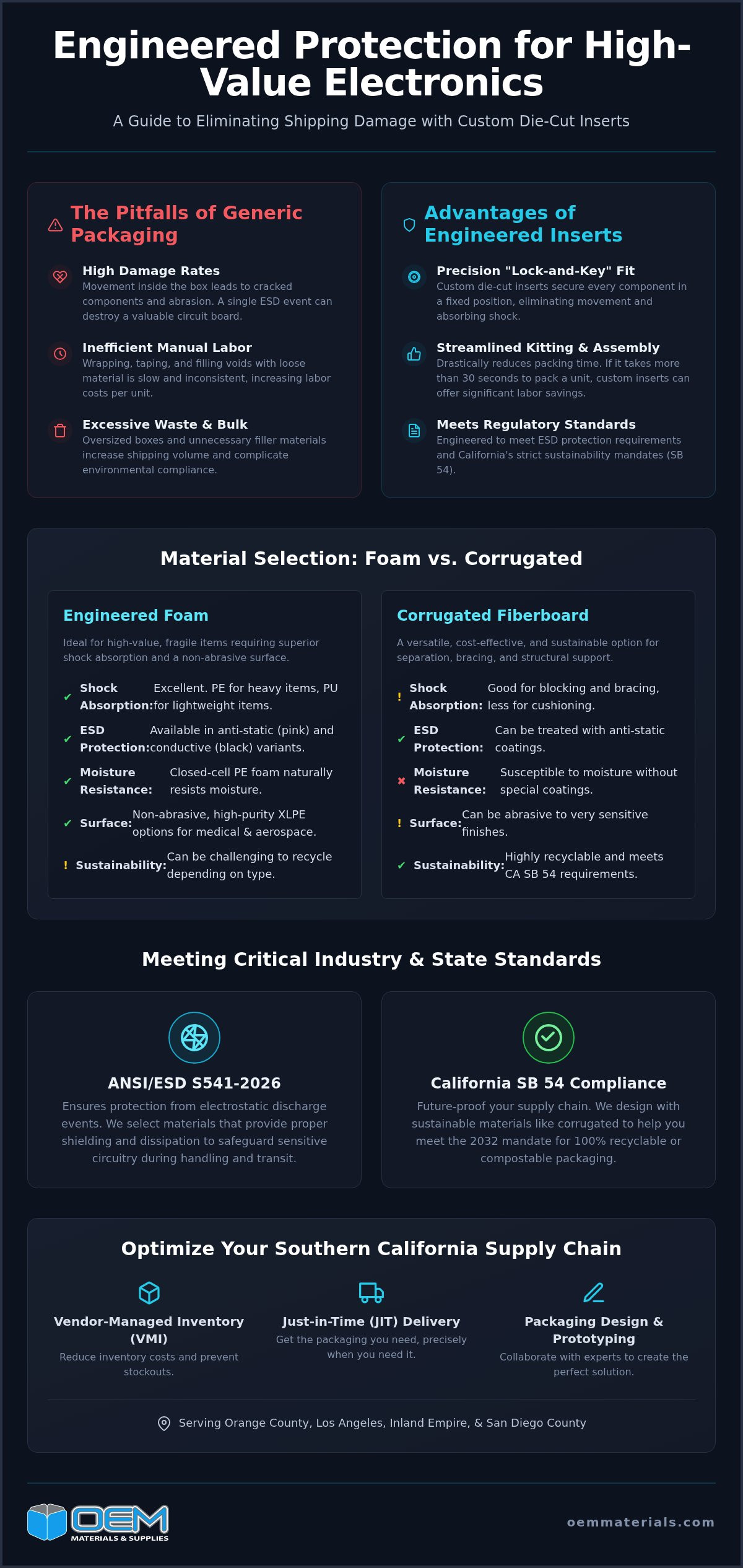
Designing for Operational Efficiency and Labor Savings
High-performance packaging should do more than just protect; it must accelerate your production line. Many manufacturers focus solely on material costs while ignoring the hidden expense of warehouse labor. Integrating custom die cut inserts for electronics directly into the assembly workflow eliminates the need for manual wrapping, taping, and “void-fill” guessing games. An intuitive, drop-in design ensures that even entry-level warehouse staff can pack a unit with 100% consistency in seconds. This standardization removes the variability that often leads to shipping damage and inconsistent customer experiences.
Engineering these inserts for multi-pack configurations also offers significant logistical advantages. By optimizing the internal geometry, you can often fit more units into a single master carton without compromising protection levels. This reduces the total shipping volume and helps mitigate the rising costs of dimensional (DIM) weight charges. A strategic custom packaging design transforms the box from a simple commodity into a tool for operational efficiency. When your packaging is engineered for speed, the savings in labor and freight often outweigh the initial tooling investment over the life of a product run.
Kitting and Pre-Assembly
Kitting services allow you to receive complete packaging sets that are ready for immediate use. Instead of managing separate inventories of boxes, foam, and static shielding bags, you receive a single SKU that includes all necessary components. This eliminates secondary operations at your facility and significantly reduces the footprint of packaging materials on your assembly floor. Improved inventory accuracy is a natural byproduct of this approach; when you use one kit per finished product, tracking your packaging burn rate becomes a simple 1:1 calculation. This level of organization is vital for high-volume factories in Orange County and the Inland Empire that operate on lean manufacturing principles.
Optimizing the Unboxing Experience
The unboxing process is the first physical touchpoint for your customer, often a technician or field engineer. A well-designed die-cut insert allows for professional, easy access to the device and its accessories without forcing the user to dig through messy loose-fill materials. For oversized electronic enclosures or server racks, using edge and corner protectors in conjunction with die-cut bases provides heavy-duty stability during the unboxing phase. This approach reduces waste and simplifies disposal for the end user, which is increasingly important as corporate sustainability mandates become more stringent. If you are ready to streamline your packing process, you can request a quote for a custom kitting solution tailored to your specific production volume.
Sourcing Die Cut Inserts in Southern California
Sourcing custom die cut inserts for electronics requires more than a simple catalog order; it demands a logistical partnership that understands the pace of industrial manufacturing. For factories in Los Angeles and Orange County, local sourcing provides a distinct advantage in both lead times and freight costs. National distributors often struggle with the specific logistical requirements of Southern California industrial zones, leading to delays that can stall a production line. Working with a local wholesale industrial packaging supplier allows for immediate design adjustments and rapid prototyping that distant vendors cannot match. This proximity ensures that your protection strategy evolves alongside your product development.
Logistics and Supply Chain Support
High-volume electronics production requires a supply chain that responds to demand shifts without delay. Implementing just-in-time (JIT) delivery programs ensures that bulky foam and corrugated inserts don’t consume valuable floor space in your facility until they are needed. You can maintain lean operations by leveraging vendor-managed inventory (VMI). This system prevents stockouts by allowing your supplier to monitor and replenish packaging levels automatically based on your actual burn rate. On-site consultations in San Diego and Riverside provide the technical support needed to refine designs as your product lines evolve. Consolidating your packaging spend with a full-service supplier also simplifies procurement by reducing the number of vendors you must manage for boxes, cushioning, and ESD materials.
Requesting a Quote for Custom Inserts
To receive an accurate engineering recommendation for custom die cut inserts for electronics, procurement teams must provide specific data points. We require precise product dimensions, the total weight of the assembly, and the fragility rating or G-factor if it has been determined through drop testing. Providing an estimate of your annual usage is equally important. This allows us to offer volume-based pricing advantages and schedule production runs that align with your forecasted needs. Accurate data helps our design team determine whether a multi-cavity die or a specific foam density is the most cost-effective choice for your specific application. If you have a new component ready for production or are experiencing damage with your current solution, contact OEM Materials for a design consultation to review your requirements.
Optimizing Your Electronics Supply Chain with Precision Engineering
Transitioning to engineered packaging is a strategic move that addresses the core challenges of modern electronics distribution. By prioritizing material density and ESD compliance with ANSI/ESD S541-2026 standards, you eliminate the high costs of shipping damage and product returns. Implementing custom die cut inserts for electronics also transforms your warehouse operations; it reduces labor through intuitive designs and kitting services that allow your team to pack faster and with greater accuracy.
OEM Materials & Supplies is a dedicated partner for manufacturers across Los Angeles, Orange County, and San Diego. Our expertise in the aerospace, medical, and electronics sectors ensures that your packaging meets rigorous industry standards while staying compliant with California SB 54 regulations. We provide full-service assembly and inventory management to streamline your production cycle and reduce overhead.
If you’re ready to improve your protection levels and operational efficiency, contact OEM Materials for a custom packaging quote. Our team is prepared to review your product dimensions and annual usage to develop a solution that delivers long-term reliability for your most sensitive components. We look forward to helping you secure your supply chain.
Frequently Asked Questions
What is the most effective foam density for heavy electronic power supplies?
High-density polyethylene (PE) foam is typically most effective for heavy power supplies. These components require a material that resists bottoming out during impact while maintaining structural integrity. A closed-cell structure provides the necessary support to distribute the weight across the entire insert. The specific density rating depends on the G-force tolerance of the unit and its total mass. Engineers calculate this to ensure the foam compresses just enough to absorb shock without failing.
How do custom die-cut inserts reduce shipping costs compared to standard boxes?
Custom die cut inserts for electronics reduce costs by optimizing the internal volume of the shipping container. By eliminating the need for excessive void-fill materials like bubble wrap or peanuts, manufacturers can often use smaller master cartons. This reduction in package dimensions directly lowers dimensional (DIM) weight charges from carriers. These inserts also enable multi-pack configurations, allowing more units to be shipped per pallet, which maximizes freight efficiency for high-volume production runs.
Can die-cut inserts be made from 100% recyclable materials?
Yes, die-cut inserts can be engineered using 100% recyclable corrugated fiberboard or specialized recyclable foams. For many Southern California electronics manufacturers, moving to corrugated-only inserts is a practical way to meet California SB 54 requirements. These designs use strategic folds and tabs to create protective air cells that mimic the cushioning properties of plastic materials. While foam is often necessary for extreme fragility, corrugated remains the gold standard for sustainability and ease of disposal.
What is the typical lead time for custom die-cut tooling and prototypes?
Lead times vary based on design complexity, but rapid prototyping typically occurs within a few business days once CAD files are finalized. Tooling for high-volume production runs usually takes one to two weeks to manufacture. OEM Materials & Supplies prioritizes speed for Southern California clients to ensure product launches remain on schedule. Once the steel rule die is complete, production cycles for custom die cut inserts for electronics are highly efficient, supporting both short runs and large-scale manufacturing programs.
How does ESD foam protect electronics differently than standard foam?
ESD foam is engineered with antistatic or conductive properties to prevent the buildup and discharge of static electricity. Standard foam can generate triboelectric charges when moved, which can instantly ruin sensitive microprocessors. ESD-safe materials are categorized by their surface resistivity, typically ranging from 10^4 to 10^11 ohms per square. These materials comply with ANSI/ESD S541-2026 standards, ensuring that high-value components remain protected from both physical impact and invisible electrical events throughout the supply chain.
Is it possible to combine foam and corrugated materials in a single die-cut insert?
Hybrid packaging designs frequently combine a corrugated frame with foam contact points to provide targeted protection. This approach utilizes the structural rigidity of corrugated boxes for weight distribution while using engineered foam only where the sensitive circuitry touches the packaging. This method is highly effective for reducing total material costs and improving recyclability. It’s a common solution for manufacturers in Orange County who need to balance rigorous protection with corporate sustainability mandates.
What information do I need to provide for a custom packaging insert quote?
To provide an accurate quote, we require the product’s physical dimensions, its total weight, and a fragility rating or G-factor. Procurement managers should also include estimated annual usage and any specific compliance requirements, such as ESD safety or cleanroom standards. Providing a physical sample or a 3D CAD model of the electronics assembly allows our design team to create a more precise fit. This data ensures the final engineering recommendation is both cost-effective and functionally sound.
How do Southern California manufacturers benefit from local VMI programs?
Local vendor-managed inventory (VMI) programs allow manufacturers in Los Angeles, San Diego, and Riverside to reduce on-site storage requirements. By keeping a buffer of custom inserts at a nearby facility, you ensure that production lines never stop due to packaging shortages. This proximity enables just-in-time (JIT) delivery, which improves cash flow by reducing the amount of capital tied up in packaging stock. It also allows for rapid response to sudden shifts in production volume.