
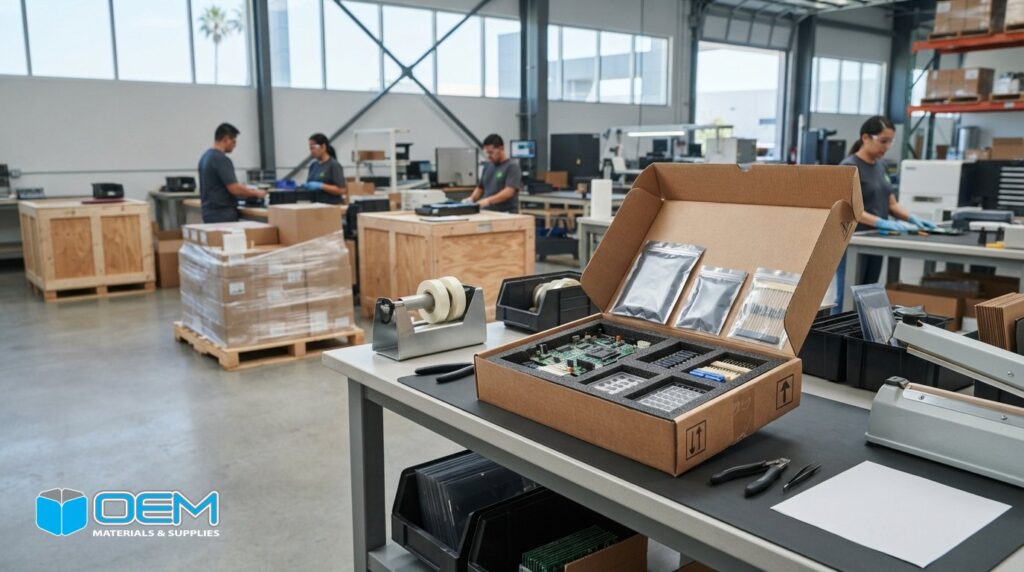
What if the electronic components that passed your final quality control checks are actually ticking time bombs destined to fail in the hands of your customers? Latent damage from electrostatic discharge often goes undetected during initial testing, only to cause catastrophic field failures weeks or months later. Selecting the right ESD packaging for sensitive components is not just about avoiding immediate sparks; it is about ensuring the long-term reliability of your high-value electronics.
You likely understand that standard bubble wrap or non-treated corrugated boxes are insufficient for protecting sophisticated circuit boards and semiconductors. However, the complexity of ANSI/ESD S20.20 standards and the high cost of over-packaging can make procurement a significant challenge. This guide explains how to select and implement the correct electrostatic discharge packaging to eliminate shipping damage while maintaining strict compliance. We will examine the differences between conductive and dissipative materials, the benefits of custom foam inserts, and how a local vendor-managed inventory partner in Southern California can streamline your operations and reduce supply chain delays.
Key Takeaways
- Understand the critical difference between immediate component failure and latent defects that cause reliability issues after products reach the field.
- Identify the correct surface resistivity requirements to choose between conductive, dissipative, and anti-static materials for your specific application.
- Learn how to combine custom corrugated boxes and foam inserts to create effective ESD packaging for sensitive components that meets ANSI/ESD S20.20 standards.
- Explore the design process for multi-component kits and rapid prototyping tailored for high-precision aerospace and medical device manufacturing.
- Discover how local vendor-managed inventory programs in Southern California can eliminate supply chain delays and optimize your warehouse space.
The Critical Role of ESD Packaging in Electronic Component Safety
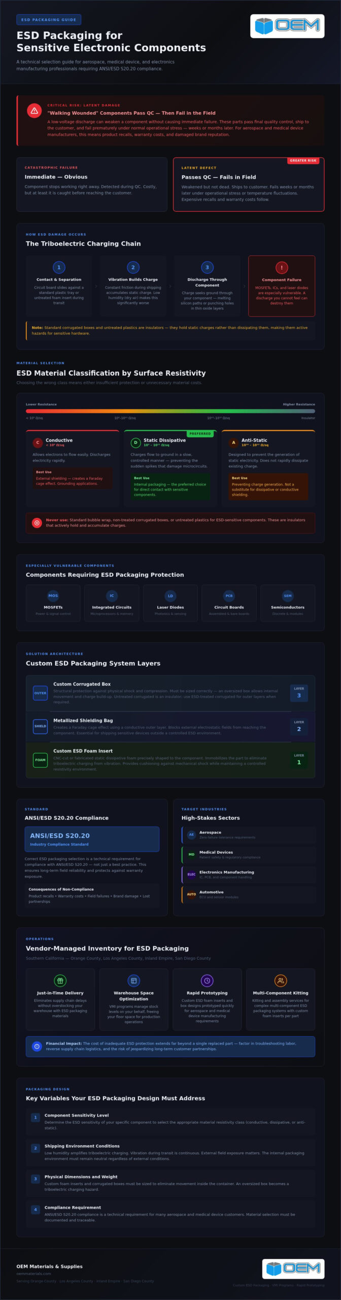
electrostatic discharge (ESD) is the sudden, uncontrolled flow of electricity between two objects with different electrical potentials. In a manufacturing or shipping environment, this usually occurs when a person or a tool touches a sensitive component. Modern microelectronics are increasingly susceptible to these events because internal circuits are microscopic. A discharge that a human cannot even feel can easily melt internal silicon paths or punch holes through thin oxide layers. Standard corrugated boxes and untreated plastics are insulators; they hold static charges rather than dissipating them. This makes them active hazards for sensitive hardware. Static is a silent killer of product reliability. It destroys margins and customer trust.
Understanding Latent Damage in Electronics
A catastrophic failure is obvious because the part stops working immediately. However, the more insidious threat is latent damage. This occurs when a low-voltage discharge weakens a component but does not cause it to fail during final quality control testing. These “walking wounded” parts pass through your facility and ship to the customer. Once in the field, normal operational stress or temperature fluctuations cause the weakened circuit to fail prematurely. For manufacturers in the aerospace and medical device sectors, these failures are unacceptable. They lead to expensive product recalls, damaged brand reputations, and high warranty costs. Implementing specialized ESD packaging for sensitive components is a technical requirement for compliance with ANSI/ESD S20.20 standards and ensures long-term field reliability.
The Mechanics of Triboelectric Charging
Static electricity is primarily generated through triboelectric charging. This happens when two materials contact and then separate, such as a circuit board sliding against a standard plastic tray or a foam insert inside a shipping container. Vibration during transit creates constant friction, building up a charge that eventually seeks a path to ground through your component. Environmental factors like low humidity exacerbate this problem because dry air acts as an insulator, allowing higher charges to accumulate on surfaces. Components like MOSFETs, integrated circuits, and laser diodes are particularly vulnerable to these spikes. Effective custom packaging design must account for these variables to ensure the internal environment remains neutral regardless of external shipping conditions. Using the right ESD packaging for sensitive components prevents the accumulation of these dangerous charges from the moment the part leaves the assembly line.
The financial consequences of inadequate protection extend far beyond the cost of a single replaced part. Consider the labor involved in troubleshooting field failures and the logistics of reverse supply chains. In high-stakes industries, a single failure can jeopardize a long-term partnership. Professional-grade materials provide the necessary shield to protect your high-value electronics from the warehouse to the end user.
Decoding ESD Material Standards: Conductive vs. Dissipative vs. Anti-Static
Not all static-safe materials offer the same level of protection. Understanding the hierarchy of surface resistivity is essential for selecting the correct ESD packaging for sensitive components. Industry professionals classify these materials into three primary categories based on how quickly they allow electrical charges to move across their surfaces. Choosing the wrong class can lead to either insufficient protection or unnecessary material costs.
Conductive materials have the lowest resistance, typically measuring less than 10^5 ohms per square. They allow electrons to flow easily, which makes them ideal for grounding applications. Because they discharge electricity rapidly, they are often used as an external shield to create a Faraday cage effect. Static dissipative materials measure between 10^5 and 10^11 ohms per square. These are generally the preferred choice for internal packaging because they allow charges to flow to ground in a slow, controlled manner, preventing the sudden spikes that damage microcircuits. Anti-static materials, often measuring 10^10 to 10^12 ohms per square, are designed to prevent the generation of static electricity caused by friction. While they do not provide a shield against external fields, they ensure the packaging itself does not become a source of static.
Surface Resistivity and Industry Standards
Surface resistivity is measured in ohms per square, a technical metric describing electrical resistance across the surface of a material. Compliance with ANSI/ESD S20.20 and MIL-STD-1686 requires rigorous testing to ensure materials fall within these specified ranges. Engineers use specialized surface resistivity meters to verify these ratings during regular quality audits. If you are unsure which standard your current supplies meet, you can request a quote for a comprehensive packaging evaluation to ensure your facility remains compliant.
Selecting Material Based on Component Sensitivity
Matching the material class to the specific ESD Sensitive (ESDS) rating of your part is a critical engineering step. For highly sensitive components with low voltage thresholds, a dissipative material or a multi-layered shielding bag is necessary. In contrast, less sensitive items might only require anti-static bags to prevent charge buildup during transit. It is also vital to distinguish between permanent ESD properties and topical coatings. Topical treatments can wear off or wash away over time, leaving your components vulnerable. We recommend utilizing foam packaging with inherent dissipative properties for long-term storage and repeated handling. This ensures that the ESD packaging for sensitive components maintains its protective integrity throughout the entire supply chain, from the assembly line to the end user.
Essential Types of ESD Packaging for Sensitive Components
Implementing an effective static control program requires a combination of different material formats to address both electrical and physical threats. While the material standards discussed previously define the electrical properties, the physical form of the packaging determines how well it handles the rigors of the supply chain. A comprehensive system of ESD packaging for sensitive components often utilizes a nested approach, combining outer shielding with internal cushioning to provide 360-degree protection.
ESD Corrugated and Die-Cut Solutions
Custom corrugated containers serve as the primary outer defense for bulk transport. Standard cardboard is an insulator that can generate and hold significant charges. In contrast, custom corrugated boxes designed for electronics utilize conductive liners or dissipative coatings. These materials create a Faraday cage effect, which redirects external electrical fields around the exterior of the box rather than through the internal components.
Precision die-cut designs offer a significant advantage for high-volume manufacturing in Southern California. By engineering the box to the specific dimensions of the product, you can incorporate self-locking tabs and internal dividers that eliminate the need for excessive tape or fasteners. This reduces material waste and speeds up the packing process on the assembly line. For manufacturers in Orange County and Los Angeles, these custom designs ensure that sensitive circuit boards remain stationary and protected throughout local and national transit.
Engineered ESD Foam for Vibration Dampening
Cushioning is necessary to prevent mechanical damage from drops and vibration. However, standard foam is one of the most prolific generators of triboelectric charging. Professional industrial foam packaging is available in two primary ESD variants: pink anti-static and black conductive foam. Pink anti-static foam, typically made of polyurethane or polyethylene, is treated with a chemical agent that prevents the buildup of static. It is a cost-effective solution for short-term cushioning.
Black conductive foam is impregnated with carbon, providing a permanent path to ground. This material is essential for high-value components where long-term reliability is non-negotiable. When selecting foam, engineers must match the density to the weight and fragility of the PCB. A foam that is too soft will bottom out during an impact, while foam that is too rigid will transfer the shock directly to the solder joints.
Beyond boxes and foam, the system is completed with specialized bags and identification tools. Shielding bags provide a metalized layer to block electrostatic fields, while moisture barrier bags protect against humidity in long-term storage. Every package must be clearly marked with ESD labels and sealed with anti-static tape. This ensures that warehouse personnel recognize the sensitive nature of the contents before they are handled. Combining these elements into a single kit creates a robust environment for your ESD packaging for sensitive components, ensuring they arrive at their destination in factory-perfect condition.
Engineering Custom ESD Solutions: Beyond the Off-the-Shelf Box
Off-the-shelf solutions frequently lead to compromised protection or excessive material waste. When you rely on generic sizes, you often find yourself using too much filler or settling for a fit that allows the component to shift during transit. Engineering custom ESD packaging for sensitive components involves a holistic approach that treats the box and the insert as a single protective system. This integration is vital for high-precision sectors like aerospace and medical device manufacturing, where even a microscopic fracture from vibration can lead to a field failure. By designing the packaging around the specific geometry of the part, you ensure that dissipative properties and mechanical cushioning work in tandem.
Designing for Assembly and Kitting
Custom kitting streamlines the assembly line by providing technicians with a pre-configured set of materials. This eliminates the guesswork involved in selecting the right foam or bag, which significantly reduces labor costs and human error. For example, a medical device manufacturer in San Diego County recently transitioned from individual components to a fully integrated ESD kit. This change standardized their packing process and nearly eliminated the damage previously caused by inconsistent packing techniques.
Effective kit design also focuses on the end-user experience. We create custom inserts that facilitate easy component extraction, preventing technicians from having to pry parts out of tight foam cavities. This reduces the risk of physical stress on delicate solder joints and connectors. When you optimize the internal layout of the kit, you don’t just protect the product; you improve the efficiency of your entire fulfillment operation.
Prototyping and Testing ESD Packaging
Prototyping is the most critical phase for high-value electronics. We utilize custom packaging design services to create prototypes that undergo rigorous validation before full-scale production begins. This process includes drop testing and vibration analysis to ensure the custom foam remains effective under real-world shipping stresses. It isn’t enough for a material to be static-safe on the bench; it must maintain its performance after being subjected to the heat and humidity of a long-haul shipping container.
Validating ESD performance throughout the entire supply chain involves testing the surface resistivity of the prototypes after they have been stressed. This ensures that the dissipative properties aren’t just a surface treatment that wears away. For manufacturers in Riverside and Orange County, this level of engineering precision provides the data necessary to meet strict aerospace and medical compliance audits. If your current packaging hasn’t been engineered specifically for your components, you may be overspending on materials that offer inferior protection. To see how a custom-engineered system can improve your reliability, request a prototype evaluation for your most sensitive assemblies.
Implementing an ESD Packaging Strategy with a Southern California Partner
Southern California is a hub for aerospace and medical electronics manufacturing. Sourcing ESD packaging for sensitive components locally isn’t just about convenience; it’s a strategic move to stabilize your supply chain. Manufacturers in Orange County and Los Angeles face high warehouse costs and tight production schedules. Relying on out-of-state vendors for specialized ESD corrugated or custom foam often leads to delays that halt assembly lines. Local sourcing ensures that your protective materials arrive exactly when your production schedule demands them, eliminating the friction of long-distance logistics.
Local Support for San Diego and Riverside Manufacturers
Proximity allows for a level of service that remote vendors cannot match. We provide on-site consultations to identify packaging inefficiencies directly on your factory floor. This hands-on approach helps us design kits that use less material while providing superior protection. By utilizing Vendor Managed Inventory services, facilities in Riverside and San Diego can significantly reduce their lead times. We monitor your stock levels and replenish them based on your actual usage, ensuring that critical ESD supplies are always available when production ramps up.
For operations in the Inland Empire, warehouse space is a premium asset. Our Just-in-Time delivery model allows you to receive only what you need for the current production cycle. This reduces warehouse overhead and frees up valuable floor space for manufacturing equipment rather than stacks of empty boxes. Stabilizing your inventory through a local partner prevents the administrative burden of constant reordering and tracking.
Achieving Long-Term Cost Savings in ESD Packaging
Cost-effective packaging is not simply about finding the lowest price per unit. It is about selecting the material that prevents a million-dollar product failure in the field. Balancing material costs with the risk of latent damage is the key to a sustainable strategy. VMI programs prevent the hidden costs of emergency shipping and production shutdowns caused by inventory stockouts of critical ESD materials. When your packaging is managed professionally, your team can focus on core manufacturing goals rather than tracking box counts.
To begin optimizing your protection strategy, we recommend a technical consultation to review your current specifications. When requesting a quote for custom ESD packaging for sensitive components, please provide your specific product dimensions, weight, and estimated annual usage. This data allows our engineering team to develop accurate custom ESD prototypes and volume pricing tailored to your operational requirements. Contact us today to schedule an evaluation and secure your high-value electronics for transit.
Securing Your Supply Chain Against Electrostatic Discharge
Protecting high-value electronics requires an engineered approach that integrates electrical resistivity with mechanical durability. Effective ESD packaging for sensitive components is not a commodity purchase but a technical requirement for maintaining product reliability and brand reputation. By selecting materials that match your specific sensitivity ratings and utilizing custom-engineered inserts, you eliminate the risk of latent defects and costly field failures. This precision ensures that your assemblies remain compliant with ANSI/ESD S20.20 standards from the assembly line to the end user.
OEM Materials & Supplies supports aerospace and medical OEMs across Southern California with AS9100 compliant material sourcing and specialized design expertise. Our local VMI and JIT delivery options in Orange County, Los Angeles, and the Inland Empire are specifically designed to reduce warehouse overhead while preventing inventory stockouts. We provide the stability and technical support needed to manage complex industrial requirements without the delays of out-of-state shipping.
To receive a technical evaluation and accurate volume pricing, contact OEM Materials & Supplies for a custom ESD packaging consultation today. Providing your specific product dimensions, weight, and annual usage allows our engineers to develop a prototype that meets your exact needs. We are ready to help you optimize your packaging and protect your bottom line.
Frequently Asked Questions
What is the difference between anti-static and ESD shielding bags?
Anti-static bags prevent static generation but do not provide a shield against external electrical fields. They are typically pink and treated with a topical agent. ESD shielding bags contain a metalized layer that creates a Faraday cage, blocking external discharges from reaching the component. For high-value electronics in Los Angeles or Orange County, shielding bags are necessary for transport outside of protected environments, while anti-static bags are often used for internal parts storage.
How long does ESD packaging last before it loses its effectiveness?
The lifespan of your packaging depends on whether the ESD properties are topical or inherent. Topical anti-static treatments on pink poly bags and foam can degrade within six to twelve months as the chemical agents migrate or wear off. In contrast, carbon-loaded conductive materials and dissipative corrugated boxes provide permanent protection that does not expire. We recommend that manufacturers in Riverside and San Diego perform regular surface resistivity audits to ensure their inventory remains compliant with industry standards.
Do I need ESD packaging for components that are already mounted on a board?
Populated circuit boards require the same level of protection as individual components. Even when mounted, sensitive items like MOSFETs and integrated circuits remain vulnerable to discharges through the board’s conductive traces. These traces can act as a path for static to reach internal silicon structures. Using professional ESD packaging for sensitive components ensures that fully assembled boards are protected from triboelectric charging and external fields during transit between Southern California facilities or to the end customer.
Can I reuse ESD foam and corrugated boxes for multiple shipments?
You can reuse certain materials if they maintain their physical integrity and electrical properties. Carbon-loaded black foam and heavy-duty conductive plastic pallets are designed for multiple cycles. However, standard ESD corrugated boxes and pink anti-static foam often degrade with use. Contamination from oils, dust, or moisture can alter surface resistivity over time. For high-volume operations in the Inland Empire, we suggest a VMI program to manage the replacement of worn materials and ensure constant protection levels.
What are the surface resistivity requirements for dissipative packaging?
Dissipative materials must maintain a surface resistivity between 10^5 and 10^11 ohms per square. This specific range is engineered to allow electrical charges to flow to ground at a slow, controlled rate, preventing the rapid discharge that causes component melting. It’s the industry standard for internal packaging layers. When sourcing ESD packaging for sensitive components in Orange County, always verify these measurements with a calibrated surface resistivity meter to ensure the materials meet your specific engineering requirements.
How does humidity affect the performance of ESD packaging materials?
Low humidity significantly increases the risk of static generation because dry air acts as an insulator. Many topical anti-static materials actually rely on pulling moisture from the air to create a dissipative surface. In the dry climates of Riverside or the Inland Empire, these materials can lose effectiveness. For these environments, we recommend using inherent conductive or dissipative materials that do not depend on environmental humidity to maintain their electrical properties and protect your sensitive hardware.
What are the best practices for labeling ESD sensitive shipments?
Effective labeling requires placing standardized ESD caution symbols on the exterior of all shipping containers and internal bags. These yellow and black labels must be visible before the technician opens the package. This warning ensures that the contents are only handled at a grounded, ESD-safe workstation. Proper identification is a critical part of a compliance strategy for aerospace and medical manufacturers in San Diego, preventing accidental damage from ungrounded personnel during the receiving and inspection process.
Is custom ESD foam more expensive than standard protective foam?
The raw material cost for ESD-treated foam is typically higher than standard polyurethane cushioning. However, custom-engineered ESD packaging for sensitive components often results in long-term savings by reducing material waste and eliminating the high costs of product returns. A custom insert ensures a perfect fit, which reduces the labor required for packing and minimizes the risk of mechanical damage. For manufacturers in Los Angeles, this engineered efficiency often offsets the initial material price difference through improved supply chain reliability.